

India’s Solar Wafer Expansion Faces Utilization and Cost Challenges: Interview
High financing costs and polysilicon import dependence pose challenges for domestic manufacturers
October 23, 2026

Follow Mercom India on WhatsApp for exclusive updates on clean energy news and insights
India’s planned expansion of solar ingot and wafer manufacturing capacity could lead to oversupply unless production growth aligns with domestic demand and exports.
Agastya Energy has announced plans to invest approximately ₹78 billion (~$826.46 million) in a 12 GW ingot and wafer manufacturing facility at Orvakal in Kurnool, Andhra Pradesh. The project is expected to generate more than 3,500 jobs and complement the company’s planned 5 GW solar cell and module manufacturing capacity.
With India’s ingot and wafer capacity projected to reach approximately 80 GW by June 2028, manufacturers face challenges related to capacity utilization, production costs, import dependence, and global competitiveness.
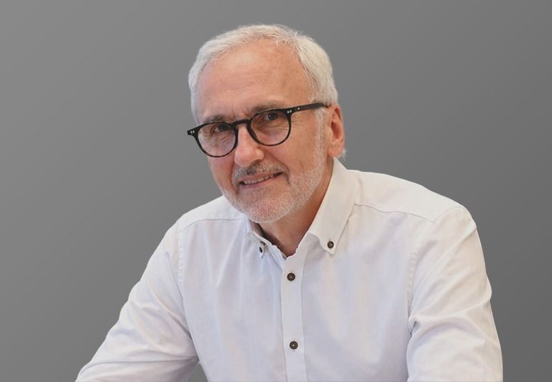
In an interview with Mercom India, Bernhard Rack, CEO of Agastya Energy, discussed the risks of overcapacity, cost disadvantages compared with Chinese manufacturers, the implications of ALMM List-III, and India’s prospects as a solar wafer exporter.
With India’s ingot and wafer capacity expanding ahead of the 2028 ALMM mandate, is there a risk of oversupply? What utilization would a 12 GW facility need to remain globally competitive?
Yes, the risk is real. Official projections point to around 80 GW of ingot and wafer capacity by June 2028. The demand that matters is operating cell capacity that can qualify and consume those wafers, and that is ultimately bound by installations and exports. India installed a record of nearly 45 GW last financial year. We have watched module capacity run ahead of demand; we should not repeat that upstream.
Ingots and wafers are far more capital-intensive than modules, so utilization decides everything. To be globally competitive, a 12 GW plant needs to run consistently at 80–85% of saleable output. At 60%, fixed cost per watt is 50% higher than at 85%.
Where will the biggest cost gaps between Indian and Chinese wafers remain, and what would it take to close them?
Not in labor, and over time, not in yield. Indian engineers will close the yield and silicon-consumption gaps within a few years of running. Learning curves can be climbed.
The gaps that persist are structural: the cost of capital, the cost of power and the depth of the supplier ecosystem. Chinese producers finance plants more cheaply, run pullers on low-cost power and source consumables nearby. Buying the same equipment does not buy the same operating economics. Closing the gap needs round-the-clock renewable power at competitive tariffs, long-tenor financing for upstream assets and consumables localized around manufacturing clusters.
Which upstream inputs will India continue to import despite localizing ingot and wafer manufacturing? Which dependency poses the greatest strategic risk?
Localizing ingots and wafers moves the dependency upstream; it does not remove it. In the near term, almost all polysilicon, most quartz crucibles, diamond wire and the bulk of pullers and wire saws will be imported, largely from China. Graphite parts and process gases are easier to localize.
The biggest strategic risk is polysilicon. It is the largest single cost input; India has no commercial production yet, and more than 90% of global supply sits in one country. It also determines traceability. Close behind is equipment: a puller without spare parts and service support is an expensive idle asset.
How can manufacturers future-proof a 12 GW facility against evolving wafer sizes, thicknesses, and cell technologies?
The semiconductor industry learned, in the move from 200 mm to 300 mm, that the wrong format can strand an entire fab. In solar, the lock-in sits mainly in the hot zone and ingot diameter, less in slicing.
The principles are simple. Choose pullers that can grow the larger diameters the roadmap points to, so today’s formats and tomorrow’s come from the same platform. Go thinner where saleable yield and cell performance justify it, not for silicon savings alone. Design for quality, because back-contact and tandem cells will demand longer lifetimes and tighter oxygen control. Building in phases lets each tranche take the latest equipment.
Where will the first major supply-demand mismatch emerge in India’s solar manufacturing value chain, and how will it affect margins?
The first mismatch is already here, in modules: well over 200 GW of nameplate capacity running at roughly 35–40% utilization. Cells are next. Capacity is expected to grow from about 35 GW to as much as 100 GW within a year, turning today’s shortage into a surplus faster than many expect. Wafers could follow around 2028–29 if every announced project is built. Polysilicon is the exception: too little supply, not too much.
Margins move to the scarce link. Today that is cells. As cell capacity arrives, that premium will narrow and margin will shift upstream to wafers for a period, even while modules stay oversupplied.
Could ALMM List-III increase domestic wafer prices? How much of a premium over imports can manufacturers absorb before project economics are affected?
In the first year or two, yes. Early supply will be concentrated, plants will still be ramping yields, and much of the first capacity belongs to integrated groups that will use it themselves.
But perspective matters. At today’s prices, wafers are well under a tenth of the price of a domestic-content module, so even a 20–25% wafer premium adds only 2-3% at module level. The real risk is stacking, where premiums on wafers, cells and modules compound into project tariffs. What the market can absorb depends on discipline across the whole chain.
Will the requirement for three independent manufacturers with a combined 15 GW capacity under ALMM List-III adequately address supply concentration concerns?
The threshold is a sensible safeguard. The initial List-III will not be issued until at least three independent units with a combined 15 GW are available, so the mandate cannot bite on a single-supplier market.
But eligibility is not availability. With cells, most listed capacity is captive and only a small fraction reaches the open market. Wafers could follow the same pattern, so merchant availability is the number to watch in the first year.
Which operating metrics will determine whether Indian ingot and wafer manufacturing can compete globally without regulatory protection?
Three numbers. First, silicon consumption per saleable watt. It captures yield, kerf loss and wafer thickness together, and since polysilicon is the largest cost item, this is where competitiveness is won or lost. Second, puller productivity: kilograms per puller per day, and how many ingots each crucible delivers. Third, energy cost per kilogram, combining consumption and tariff.
The honest test is simple: could the plant sell profitably at import parity if List-III disappeared tomorrow? If not, the regulation is carrying the business.
What must India do to become a competitive solar wafer exporter, and where could its first major export opportunities emerge?
Capacity is necessary but not sufficient. We need non-Chinese polysilicon because traceability is what export customers will pay for. We need quality proven over years, because cell makers qualify wafer suppliers slowly. And we need power and financing costs closer to global benchmarks.
On price alone, Indian wafers will not undercut Chinese wafers for some years. But markets are no longer purely open. The United States is adding cell capacity far faster than wafer capacity, and the new duties on Indian cells and modules make wafers the more credible export product. The first customers will be overseas cell makers seeking a qualified second source with traceable supply.


Arjun Joshi
More articles from Arjun Joshi.